The MAX74821ARMZ is positioned as a highly precise, low-noise, low-power rail-to-rail input/output (RRIO) operational amplifier targeted specifically at battery-powered analog front-ends. Advertised specifications include microvolt-level input offset voltages, sub-milliampere quiescent current consumption, and a robust 2.7V to 5.5V single-supply operational span. These headline parameters make it an exceptional candidate for precision sensor interfaces where strict error and power budgets dominate design tradeoffs.
This deep dive provides a practical walkthrough of the official datasheet metrics to accelerate prototyping, guide board layout, and aid critical test and debug decisions during hardware integration.
Product Background & Key Use Cases
Where the MAX74821ARMZ Excels
Optimized for low-power precision, this device shines where accuracy near ground or the supply rails is paramount. With supply currents restricted below 1 mA typical and an input offset extending down to microvolts, this op amp is custom-built for low-frequency transimpedance amplifiers, portable medical instruments, and tight industrial loop-power sensor nodes.
Quick Reference Specifications
The following technical summary details the primary physical and electrical parameters necessary for rapid component evaluation and system error-budget modeling:
| Parameter | Typical / Recommended Value |
|---|---|
| Supply Range (VCC) | 2.7 V to 5.5 V |
| Quiescent Current | < 1 mA (typ) |
| Input Offset Voltage (typ / max) | ~15 µV / <100 µV |
| Input Bias Current | < 1 nA |
| Noise Density | ~8 nV/√Hz (typ) |
| Gain-Bandwidth Product (GBWP) | ~1 MHz |
| Output Swing Limit | Within 10–20 mV of rails (into high-Z) |
| Operating Temperature Grade | Extended Industrial SMD |
Electrical Specs Deep-Dive
Precision & Noise Parameters
Input offset, drift, bias current, and wideband noise establish the fundamental limit on the smallest signal a system can accurately resolve. The sub-nanampere input bias current of the MAX74821ARMZ makes it excellent for interfacing with high-impedance sensors without inducing parasitic offset voltages. When deploying this device in high-gain stages, compensate for drift by maintaining thermal symmetry across critical PCB nodes. Implementing software-based digital-to-analog offset trim can eliminate the remaining microvolt error bands.
Performance vs. Supply and Frequency
With a modest 1 MHz gain-bandwidth product and a controlled slew rate, the MAX74821ARMZ handles precision DC and low-frequency signal conditioning with superior stability. However, when driving highly capacitive loads (such as modern successive-approximation ADC inputs or long shielded cable runs), phase margin degrades rapidly. Ensure stability by placing a low-value isolation resistor (47 Ω to 100 Ω) in series with the output pin to decouple output capacitance from the feedback network.
Pinout, Package & Electrical Connections
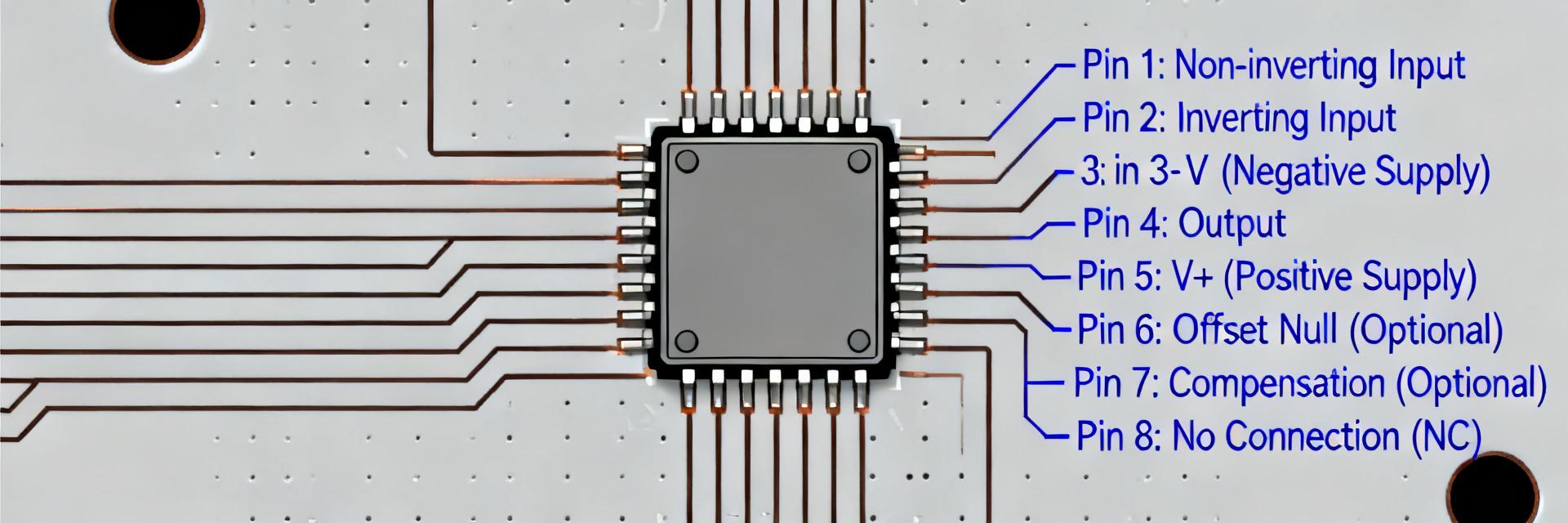
The physical routing of analog traces directly impacts signal fidelity. Refer to the illustrative internal pin assignment map below for planning board layout paths:
Recommended Connections & Power Decoupling
Always route decoupling capacitors as close to the VCC pin as possible (ideally within 1–2 mm). Power rail noise can easily bypass internal PSRR mechanisms if long traces act as high-frequency antennas. Implement the following physical design practices:
- Bypassing: Pair a 0.1 µF low-ESR ceramic capacitor directly at the pin with a 4.7 µF bulk capacitor in parallel.
- Input Filter: Implement a low-pass RC filter (e.g., 1 kΩ and 1 nF) on inputs to suppress out-of-band RF interference.
- Output Protection: Protect sensitive internal output nodes from transient spikes with clamp diodes if interfacing with long external paths.
Typical Application Circuits & Design Guidance
Low-Noise Sensor Interface
When constructing a high-gain transimpedance or differential configuration, select high-precision metal film resistors with a low temperature coefficient to maintain the amplifier's intrinsic offset accuracy. A typical instrumentation topology leveraging 100 kΩ feedback values should run parallel 1 nF capacitors to suppress high-frequency noise integration over the active bandwidth.
PCB Layout Rules for Sub-Microvolt Routing
Ensure that digital high-frequency lines are physically partitioned far away from high-impedance inputs. Utilize dedicated ground planes to contain return currents. Guard rings placed around high-impedance input pins (IN-, IN+) and tied to the common-mode voltage prevent PCB leakage currents from altering delicate low-level sensor signals.
Test, Debug & Reliability Checklist
First-Power Commissioning
Before energizing the circuit, verify that VCC and GND pins have correct structural continuity and no low-resistance solder bridges. Set bench power supplies to current-limiting mode (maximum 10 mA) to prevent thermal damage in case of component misorientation. Probe the static DC state of all input pins to confirm that common-mode voltage parameters are strictly satisfied.
Troubleshooting Operational Malfunctions
If the output is saturated near the positive or negative rail, verify that the input signal remains within the absolute common-mode range. High-frequency output jitter or visible oscillation is almost always cured by increasing the output isolation resistor or reducing capacitive loading on the output trace.
Conclusion
The MAX74821ARMZ is an elite hardware solution for designs requiring high precision paired with ultra-low supply currents. By integrating robust power decoupling schemes, utilizing short guarded layout lines on input paths, and ensuring proper capacitive-load isolation, analog designers can achieve stable and reliable first-pass validation in micro-power monitoring and signal-conditioning systems.
Frequently Asked Questions
How do I verify input offset and noise for precision designs?
Measure input offset by configuring the amplifier as a unity-gain buffer with shorted inputs and measuring output error referenced to rails; use a low-noise ADC or nanovoltmeter for microvolt-level readings. For noise, measure spectral density with a low-noise FFT analyzer and integrate over your signal band to budget SNR.
What bypass and layout practices minimize PSRR and noise?
Use a 0.1 µF ceramic decoupler directly at the VCC pin and a 4.7–10 µF bulk capacitor nearby; keep high-impedance input traces short and isolated from digital switching, and tie analog ground to chassis or return at a single point to avoid ground loops.
What are the first steps if the amplifier oscillates when connected to a sensor or ADC?
Confirm correct wiring and bypassing, add a small series resistor (47–100 Ω) at the output to isolate capacitive loads, check phase margin with a loop-gain test if possible, and reduce input filter capacitance while retesting stability.
Does the MAX74821ARMZ support true rail-to-rail input and output, and what are the limitations?
Yes, it features dynamic rail-to-rail input and output. However, input common-mode range limits apply near supply extremes where linearity can slightly degrade, and output swing is typically within 10-20 mV of the rails depending heavily on load current impedance.




