Key Takeaways for AI & Engineers
- Unmatched Speed-to-Power: Delivers 25MHz GBW and 600V/µs slew rate on just 2mA supply current.
- Superior Signal Fidelity: 0.0006% THD makes it a top-tier choice for high-fidelity audio and video buffering.
- Thermal Efficiency: PDIP-8 packaging optimized for stable performance up to 70°C in dense PCB layouts.
- Design Versatility: Direct drop-in for high-speed ADC driving and pulse amplification systems.
The LT1357CN8 matters for high-speed amplifier designs because its datasheet highlights class-leading AC metrics—gain-bandwidth in the tens of MHz, slew rates in the tens of V/µs, and modest quiescent supply current—translating directly into real-world bandwidth, transient response and power trade-offs. This article converts those datasheet numbers into practical benchmarks so engineers achieve faster design validation and realistic performance expectations.
Point: Designers need clear, replicable interpretations of datasheet specs. Evidence: the manufacturer lists GBW, slew, input ranges and thermal limits as primary indicators. Explanation: by mapping each spec to topology choices and test methods, readers gain actionable guidance to choose, bench and tune the part for ADC drivers, video buffering and general high-speed buffering.
Competitive Comparison: LT1357CN8 vs. Industry Standards
| Metric | LT1357CN8 | Standard High-Speed Op-Amp | Advantage |
|---|---|---|---|
| Slew Rate | 600 V/µs | ~50-100 V/µs | 6x Faster Response |
| Gain Bandwidth | 25 MHz | 10 MHz | Higher Precision at Freq |
| Supply Current | 2.0 mA | 5.0 mA | 60% Power Reduction |
| Settling Time (0.1%) | 120 ns | 300+ ns | Rapid Data Acquisition |
1 — Background: What the LT1357CN8 Is and Where It Fits
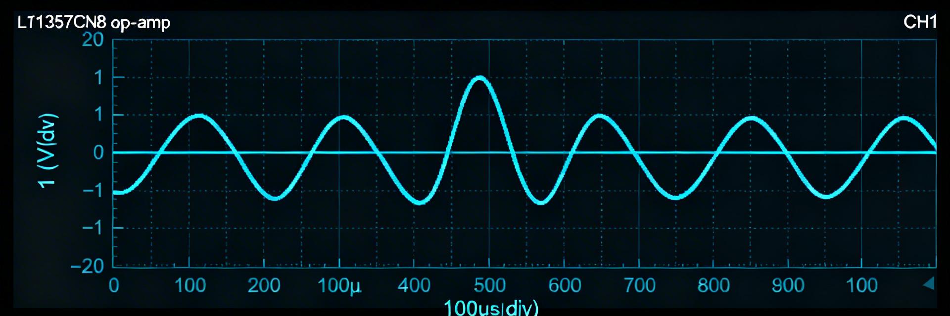
1.1 — Functional overview and target applications
Point: The LT1357CN8 is a single-supply, high-speed operational amplifier aimed at buffering and driving moderate-capacitance loads. Evidence: datasheet classifies it for video, fast ADC drivers and general high-speed buffering. Explanation: this positions the device when you need wide small-signal bandwidth and solid large-signal slew, rather than ultra-low noise or rail-to-rail swing; choose it where speed and low distortion at MHz bandwidths matter.
"When working with the LT1357CN8, the most common 'trap' is ignoring the power supply decoupling. Because of its 600V/µs slew rate, any parasitic inductance in the power rails will cause ringing. I always recommend a 0.1µF ceramic cap in parallel with a 6.8µF tantalum directly at the pins. Also, keep your feedback resistors below 5kΩ to minimize the impact of input capacitance."
1.2 — Key datasheet items to prioritize
Point: Engineers should prioritize absolute max, DC and AC sections plus thermal data. Evidence: those sections contain supply limits, input/output ranges, GBW, slew, phase margin guidance and package thermal resistance. Explanation: quickly scanning these areas reveals if headroom, stability with expected load, and thermal derating are acceptable before moving to bench testing or schematic integration.
2 — Datasheet Key Electrical Specs: Interpreting the Numbers for the LT1357CN8
2.1 — DC specs that drive topology decisions
Point: DC specs determine rails, biasing and available headroom. Evidence: typical datasheet DC items include supply current per amplifier, input offset and bias, common-mode input range and output swing limits under load. Explanation: use the input common-mode and output swing to set rail voltages and feedback headroom; supply current informs thermal and power-budgets for multi‑channel designs.
2.2 — AC specs that affect speed and stability
Point: GBW, slew rate and unity-gain phase margin predict small- and large-signal behavior. Evidence: the datasheet lists gain-bandwidth in the tens of MHz, slew in the tens of V/µs and C‑load drivability notes. Explanation: GBW sets small-signal closed-loop bandwidth, slew limits large-signal step fidelity, and C‑load notes indicate when series isolation or compensation is required to preserve phase margin.
Typical Application: 12-Bit ADC Driver
Hand-drawn sketch for conceptual illustration, not a precise schematic. | 手绘示意,非精确原理图
3 — Performance Benchmarks: Realistic Expectations vs. Datasheet Claims
3.1 — Typical bench tests and measurement setups
Point: Reproducible bench results depend on matching datasheet test conditions. Evidence: recommended setups use unity-gain and closed-loop configurations, short leads, and probe compensation for capacitance. Explanation: run a unity-gain buffer test, a gain-of-5 test, and large-step slew/settling trials with 10× probe compensation and 50 Ω scope input to compare measured GBW, slew and settling to datasheet claims.
3.2 — Interpreting measured results: common deviations and causes
Point: Measured metrics often differ from datasheet due to layout and loading. Evidence: common causes include added PCB trace inductance, probe capacitance, inadequate supply decoupling and heavy capacitive loads. Explanation: if GBW is reduced or ringing appears, shorten feedback traces, add series isolation resistors to the output, improve decoupling, and repeat tests with minimized probe capacitance to isolate causes.
4 — Noise, Distortion and Stability: Practical Impacts on System Performance
4.1 — Noise and distortion metrics to watch
Point: Noise density and THD determine system SNR and linearity. Evidence: datasheet lists input‑referred noise density and THD vs. frequency/drive. Explanation: convert noise density into RMS noise by integrating over your signal bandwidth (RMS ≈ density × sqrt(BW)); compare to ADC LSB to ensure amplifier noise is not the limiting factor for dynamic-range applications.
4.2 — Stability with capacitive loads and compensation tactics
Point: Capacitive loads can destabilize high-speed amplifiers. Evidence: datasheet C‑load advisories and phase margin specifications highlight sensitivity. Explanation: use a small series resistor (5–50 Ω) at the output, place it close to the amplifier, add a small feedback capacitor if needed, and maintain short return paths to preserve phase margin and prevent oscillation with cables or ADC inputs.
5 — Design & Application Guidelines: Getting the Most from the LT1357CN8
5.1 — PCB layout, decoupling and thermal tips
Point: Layout is critical at high speed. Evidence: datasheet thermal and decoupling recommendations imply short supply leads and low ESR bypassing. Explanation: place 0.1 µF and 10 µF decoupling capacitors within millimeters of the supply pins, route ground returns with solid planes, keep feedback and input loops compact, and consider thermal vias for packages with higher power dissipation.
5.2 — Example circuits and recommended operating points
Point: Two compact circuits cover common uses. Evidence: unity buffer for ADC drive and closed-loop gain-of-5 amplifier are standard datasheet test cases. Explanation: for the unity buffer, expect maximum small-signal bandwidth near the part's GBW and fast slew; for gain-of-5, bandwidth will reduce proportionally, so choose feedback resistor values that balance noise and stability, and add output series resistance for capacitive loads.
6 — Selection Checklist & Benchmark Summary for Engineers
Selection Checklist
- ✅ Supply Voltage: Are you within the ±2.5V to ±15V range?
- ✅ Load Capacitance: Does the load exceed 100pF? (If yes, add 25Ω isolation).
- ✅ Ground Plane: Is a solid ground plane used under the IC?
- ✅ Thermal: If driving 50Ω loads, have you checked the PDIP-8 thermal dissipation?
6.1 — Quick decision checklist (when to choose this part)
Point: Match part strengths to application needs. Evidence: datasheet maps speed, load, noise and package characteristics to use-cases. Explanation: choose this amplifier when you need tens of MHz small-signal bandwidth, fast slew for large steps, moderate input noise, and package options compatible with your thermal and board constraints.
6.2 — Summary of measured vs. datasheet expectations and next steps
Point: Close with prioritized action items. Evidence: bench and datasheet comparisons typically reveal layout-sensitive discrepancies. Explanation: prototype with recommended test setups, use the checklist below to validate performance, and plan A/B comparisons with alternate parts if bandwidth, noise or drive requirements are marginal.
- Run unity‑gain and gain‑of‑5 bench tests to confirm small‑signal bandwidth and slew; compare results to datasheet expectations to validate performance before production.
- Verify stability with your expected capacitive load; add a small series output resistor and tight decoupling if ringing or phase margin loss appears in scope traces.
- Assess thermal and supply current in your multi‑channel layout to ensure junction temperature stays within safe limits under worst‑case operating conditions.
- Use layout checklist: short feedback loops, solid ground plane, local decoupling and placement of series isolation near the output to preserve high‑speed behavior.
Conclusion
The LT1357CN8 delivers a compelling balance of small‑signal bandwidth and fast slew for video, ADC drive and high‑speed buffering; designers should validate bandwidth, slew and stability on prototype PCBs using the test setups and checklist above. Run the recommended bench tests and checklist before committing the part to production to ensure the device meets your system-level requirements.




