Point: A quick, data-driven snapshot frames why this part is relevant for precision current measurement. Evidence: The device lists an input common-mode range near −2 V to 42 V, selectable gains of 20/50/100 V/V, a small-signal bandwidth of about 650 kHz, PSRR and CMRR performance tailored for shunt sensing, and a specified settling time near 6.5 μs. Explanation: This article translates those headline datasheet numbers into concrete design trade-offs for accuracy, speed, noise, and PCB layout.
Point: The goal is practical design guidance rather than verbatim datasheet recitation. Evidence: Throughout, key electrical specs are interpreted into formulas, bench checks, and selection rules engineers can apply immediately. Explanation: Readers will get worked examples for offset-to-current conversion, CMRR effects at high common-mode voltages, noise budgeting, and a concise test checklist to validate performance on the bench.
1 — Quick background: what the INA187A2IDBVR is and where it's used
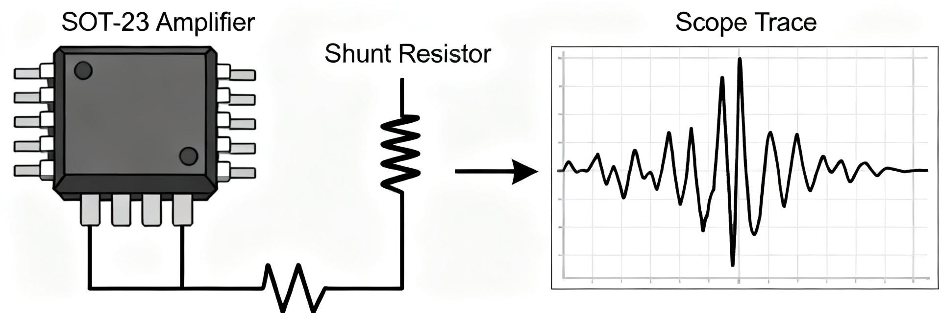
Point: Define the device in one sentence and list typical use cases. Evidence: The INA187A2IDBVR is a high-precision current sense amplifier suitable for low-side and high-side shunt measurement and bi-directional sensing. Explanation: It targets battery management, power-supply current monitoring, and motor-control feedback where low offset and good common-mode rejection are required.
Part overview & variants
Point: Summarize device variants, gains, and package. Evidence: The family offers selectable fixed gains (20, 50, 100 V/V) in a compact SOT-23-6 package and supports broad supply/common-mode operation. Explanation: These options let designers trade sensitivity vs. bandwidth and fit the amplifier into space-constrained power designs while preserving compatibility with typical ADC input ranges.
At-a-glance datasheet table
| Parameter | Typical / Max | Datasheet Location |
|---|---|---|
| Supply / common-mode range | ≈ −2 V to 42 V | Electrical characteristics |
| Gains | 20 / 50 / 100 V/V | Ordering/options |
| Small-signal bandwidth | ~650 kHz | Frequency response |
| Input offset (typ / max) | low μV to few 100 μV | Input offset specs |
| Offset drift | specified μV/°C | Thermal characteristics |
| CMRR / PSRR | High, specified in dB | Rejection specs |
| Input-referred noise | nV/√Hz | Noise characteristics |
| Settling time | ~6.5 μs to specified error | Transient response |
| Supply current | low mA range | Supply current table |
2 — DC accuracy: offset, gain, CMRR and their practical impact
Input offset, offset drift and calibration implications
Point: Offset and drift set the baseline error floor for DC current measurements. Evidence: The datasheet specifies typical and worst-case input offset plus temperature coefficient; these translate directly to current error via the sense resistor. Explanation: Use the simple conversion below to quantify error and determine whether calibration or offset-trimming is required for your target accuracy.
Formula: I_error ≈ V_offset / R_shunt
Example: a 100 μV offset across a 50 mΩ shunt yields 2 mA error. For a 1 A measurement that is 0.2% error; for a 100 mA range it becomes 2% error. Apply offset drift across operating temperature to determine worst-case calibration intervals.
CMRR & gain error across common-mode range
Point: CMRR and gain error determine how common-mode voltage degrades accuracy. Evidence: The datasheet gives CMRR in dB over the allowed common-mode span; gain error is specified separately. Explanation: When the common-mode voltage is large, finite CMRR converts a fraction of that voltage into a differential error—calculate the induced error and compare to offset-derived error to choose mitigation strategies.
Worked example: with 80 dB CMRR (10,000:1), a 40 V common-mode produces up to 4 mV of apparent differential error; across a 50 mΩ shunt that is 80 mA error—unacceptable for small-signal monitoring. Solutions include lowering R_shunt, adding differential filtering, or using a front-end divider/clamp to limit common-mode excursions.
3 — Dynamic & noise performance: bandwidth, settling, PSRR
Bandwidth, slew, and settling time trade-offs
Point: Bandwidth and settling determine suitability for pulse-current measurement. Evidence: The small-signal bandwidth (~650 kHz) and datasheet settling specification (~6.5 μs) indicate response limits. Explanation: Higher gain reduces effective bandwidth; for pulsed currents ensure the chosen gain retains sufficient bandwidth to capture pulse edges. Validate on bench with step stimuli and measure time to specified error band.
Noise, PSRR and their effect on resolution
Point: Input-referred noise and PSRR define achievable resolution. Evidence: The datasheet provides noise spectral density and PSRR figures. Explanation: Integrate noise density over your measurement bandwidth to get RMS voltage noise, then convert to current noise via R_shunt to determine the smallest resolvable current.
Noise integration: V_rms = sqrt(∫ (e_n^2) df) ≈ e_n * sqrt(BW)
Example: e_n = 7 nV/√Hz over 100 kHz bandwidth gives ≈22 μV RMS; across a 10 mΩ shunt that’s ~2.2 mA RMS noise—use averaging, reduced bandwidth, or larger shunt to improve resolution.
4 — Input & protection specs, supply behavior, and thermal limits
Input protection, common-mode beyond limits, and safe operating practices
Point: Exceeding common-mode limits can trigger internal clamps or damage. Evidence: The datasheet notes protection behavior for out-of-range inputs and recommends external protection for transient events. Explanation: Add a small series resistor, RC filtering, or a TVS on the shunt path to limit fault currents and protect the amplifier from inductive transients during motor or switching events.
Supply current, thermal derating, and SOA considerations
Point: Quiescent current and package thermal resistance govern safe dissipation and spec stability. Evidence: The package (SOT-23-6) has finite θJA; supply current times supply voltage gives power dissipation. Explanation: Estimate junction rise and check if increased temperature degrades offset, drift, or PSRR; include a thermal calculation to ensure operation within derating limits.
Thermal calc: ΔT_j = P_dis * θJA; T_j = T_ambient + ΔT_j
5 — Design & measurement guide: choosing gain, shunt, and test setup
Selecting gain and shunt resistor: formulas and trade-offs
Point: A step-by-step selection minimizes saturation and maximizes ADC use. Evidence: Start from required measurable current range, select R_shunt to place sense voltage within amplifier common-mode and input limits, then pick the amplifier gain so the output uses the ADC full scale without clipping. Explanation: Example flow: required I_max → desired V_sense (e.g., 50–100 mV) → R_shunt = V_sense / I_max → choose gain so V_out = gain * V_sense ≈ ADC_FS * 0.9.
Bench test procedure and measurement checklist
Point: Validate key electrical specs with a practical procedure. Evidence: Recommended instruments include a stable current source, vector scope, precision DMM, and low-inductance shunt. Explanation: Inject DC and step currents to measure offset/drift and settling; use sine sweeps to verify bandwidth; measure RMS noise with a spectrum analyzer or integrate noise density. Check decoupling and grounding for minimum noise.
6 — Applications, common pitfalls, and a practical implementation checklist
Example applications and reference configurations
Point: Outline typical uses and their critical specs. Evidence: Battery-management needs low offset and drift; motor control emphasizes bandwidth and robust input protection; PSU monitoring values PSRR and thermal behavior. Explanation: For battery systems prioritize low offset and drift with moderate gains; for motor pulses use lower shunt and lower gain to preserve bandwidth and prevent saturation.
Implementation checklist & troubleshooting tips (actionable)
Point: Provide an actionable checklist to catch common integration errors. Evidence: Key items include verifying supply/common-mode range, computing offset-induced error, noise budgeting, layout and decoupling, and ESD protection. Explanation: If you see unexpected offset, check common-mode beyond limits and input clamps; excessive noise often traces to layout, ground loops, or missing decoupling—start by simplifying the board and re-measuring.
- Verify supply and common-mode within datasheet limits
- Compute offset → current error for your R_shunt
- Measure noise and compare to budget
- Confirm layout: short sense traces, solid return, decoupling near pins
- Validate protection: series resistor, TVS, RC where appropriate
Summary
Point: Condense the design lens takeaways. Evidence: Reading the INA187A2IDBVR datasheet with design intent clarifies which electrical specs drive real-world performance. Explanation: Focus on offset & drift, CMRR/PSRR, bandwidth/settling, and robust layout/protection; apply the formulas and checklist above to translate datasheet numbers into safe, accurate current-sensing implementations.
FAQ
How does INA187A2IDBVR offset translate into current error?
Offset converts directly via R_shunt (I_error = V_offset / R_shunt). For example, 50 μV offset across 20 mΩ equals 2.5 mA error. Consider offset drift across expected temperature range and decide whether calibration or a larger shunt is needed to meet percentage error targets.
What bench tests verify bandwidth and settling?
Use a pulse generator to create a step current into the shunt and probe the amplifier output with a high-bandwidth oscilloscope. Measure time to settle within the specified error band for settling time and use sine sweeps to find the −3 dB point for bandwidth verification. Include decoupling and probe compensation checks.
How do I protect the inputs from transients without hurting accuracy?
Use a small series resistor to limit clamp currents, a low-capacitance TVS for large transients, and RC filtering sized to preserve the measurement bandwidth. Keep added resistance minimal to avoid offset from input bias currents and compensate in calibration if necessary.
What is the small-signal bandwidth of the INA187 family and how does gain affect it?
The small-signal bandwidth is approximately 650 kHz. Selecting a higher fixed gain (such as 100 V/V) typically decreases effective closed-loop bandwidth compared to lower gain options (20 V/V or 50 V/V). Always confirm dynamic performance at your target gain configuration.




