The INA299A3IDBVR is examined here from a data-first perspective: typical quiescent current in the tens of microamps, common-mode acceptance into the high-voltage domain, CMRR on the order of multiple tens of dB, sub-percent end-to-end accuracy in well-implemented systems, and bandwidth sufficient for kilohertz to low‑hundreds of kilohertz monitoring. This piece treats the INA299A3IDBVR as the subject of a specs-driven inspection and aims to give engineers concise, actionable guidance to select, validate, and integrate this current-sense amplifier.
Point: Designers need a compact, fixed‑gain current monitor with wide common‑mode tolerance and low supply draw. Evidence: the device family targets high‑side sensing and low‑power telemetry. Explanation: the following sections translate key spec lines into bench checks, PCB layout rules, and selection tradeoffs so the component choice maps to measurable system performance.
Product Overview & Target Use Cases
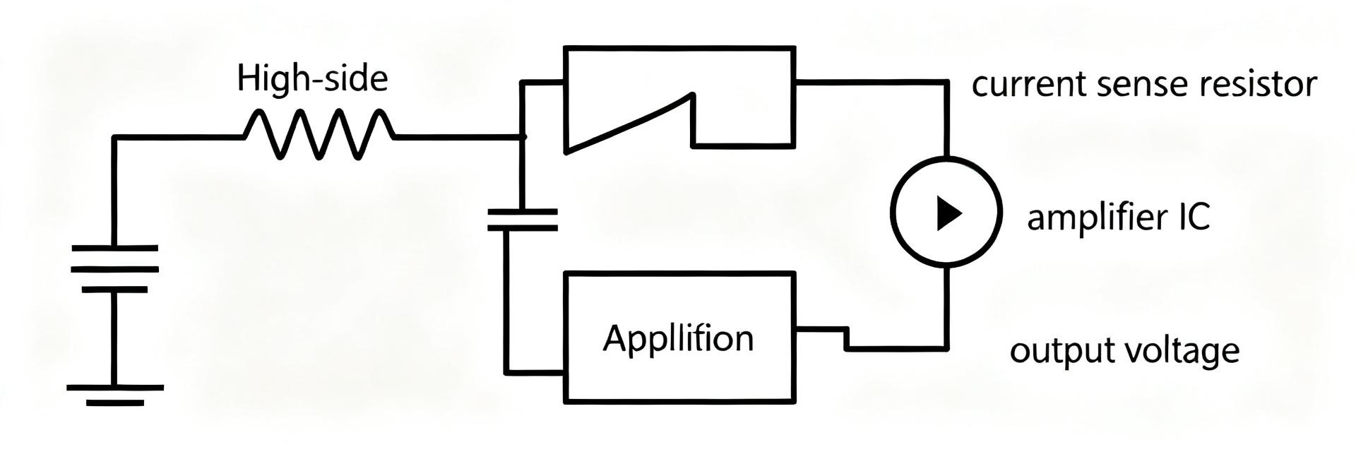
What the INA299A3IDBVR is
Point: The device is a fixed‑gain, single‑ended voltage output current-sense amplifier suited to high‑side measurements. Evidence: the A3 variant denotes a fixed gain option and a single output stage for direct ADC interfacing. Explanation: engineers should remember: fixed gain, voltage output compatible with common microcontroller ADCs, and design primarily for unidirectional current measurement in power monitoring and telemetry.
Best-fit applications
- Power rails monitoring — wide common‑mode supports rail sensing without extra level shifting.
- Battery management — low quiescent current preserves sleep budgets in multi‑cell systems.
- Motor control telemetry — bandwidth and transient response let engineers observe dynamic current events.
- Server and telecom rails — accuracy and CMRR matter for tight current budgeting and fault detection.
- Industrial monitoring — robust input envelope reduces the need for external protection networks.
Point: Check system-level constraints first. Evidence: common‑mode voltage, ADC input range, allowable shunt dissipation, and required dynamic measurement bandwidth govern suitability. Explanation: when evaluating the part, begin by confirming the maximum system bus voltage, the worst‑case shunt power, and the ADC input span to avoid surprises during integration.
Electrical Performance: Accuracy, Offset, and Noise
Key precision specs to evaluate
Point: Offset voltage, gain error, linearity, and temperature drift determine practical accuracy. Evidence: datasheet numbers convert to absolute current uncertainty via I_meas = (Vout/Gain)/Rshunt and error contributions from offset and gain. Explanation: compute worst‑case uncertainty by summing offset‑equivalent current and percentage gain error across expected shunt values to predict system accuracy at room and elevated temperatures.
Measured vs. datasheet expectations (what to validate on bench)
Point: Bench validation should target offset, gain, and noise across representative common‑mode points. Evidence: a simple test uses precision shunts, low‑noise source meter, and differential probe to capture Vout vs I_shunt across ranges. Explanation: expect datasheet typical numbers; larger deviations usually point to PCB layout, grounding errors, or unaccounted thermal gradients rather than silicon defects.
Common-Mode Range, CMRR & Input Limits
Understanding the common-mode envelope and safe operating area
Point: Common‑mode limits decide whether the amplifier can monitor high‑side rails directly. Evidence: the device accepts inputs across a broad envelope, allowing direct sensing of high bus voltages without extra level-shifters. Explanation: confirm the permitted input range and any absolute maximums; exceeding those margins risks input stage distortion or permanent damage, so include margin in selection.
CMRR, tolerances, and real-world implications
Point: CMRR in dB quantifies common‑mode suppression; translate that to error volts to see impact on current readout. Evidence: error ≈ Vcm / 10^(CMRR/20) — at typical Vcm values this converts to microvolt‑level or millivolt‑level offsets. Explanation: use that converted error to evaluate whether CMRR contributes meaningfully versus offset/gain error at your shunt sizes and currents.
Bandwidth, Slew Rate & Transient Response
How bandwidth and slew rate affect measurement fidelity
Point: Bandwidth and slew define how faithfully fast current transients are captured. Evidence: limited amplifier bandwidth or slow slew with aggressive filtering will attenuate or slow edges, underestimating peak current. Explanation: choose shunt and RC filters such that the corner frequency preserves the fastest expected event while limiting noise for the ADC sampling rate chosen.
Designing for stability: output filtering and load drive
Point: Output drive and filtering interact; excess capacitance can create ringing or added settling time. Evidence: datasheet output‑drive limits and recommended load conditions guide RC placement. Explanation: place a minimal series resistor before any capacitive load, use small output capacitors for anti‑aliasing, and validate step response on scope to confirm no instability is introduced.
PCB Integration & Thermal Considerations
Layout and placement best practices
Point: PCB routing dominates real‑world offset and noise. Evidence: sense traces length, return path quality, and shunt proximity affect parasitic voltages. Explanation: place the shunt close to the amplifier inputs, run short Kelvin traces, avoid crossing noisy power planes, and add local decoupling close to the device to minimize injected disturbances and measurement error.
Power dissipation and thermal drift mitigation
Point: Shunt and amplifier dissipation create thermal gradients that shift offset and gain. Evidence: shunt power = I^2·Rshunt, and nearby copper area or vias alter thermal coupling. Explanation: use ample copper pour for shunts, thermally isolate sensitive traces from hot components, and consider calibration across temperature or choose larger shunt or remote sensing to manage drift.
Comparative Notes, Real-World Examples & Troubleshooting
Short comparative checklist
Point: Choose this device when low quiescent, fixed gain, and wide input range priority align. Evidence: metrics to weigh include quiescent current, maximum Vcm, guaranteed accuracy, and bandwidth. Explanation: if ultra‑wideband transient capture or programmable gain is required, compare alternatives; otherwise, this fixed‑gain approach simplifies ADC interfacing and calibration.
Quick troubleshooting checklist and hands-on fixes
Point: Systematic checks speed root‑cause resolution. Evidence: common symptom→cause→fix mappings include offset drift→thermal coupling→add copper or relocate hot parts; noisy readings→poor routing→shorten leads and add ground plane. Explanation: follow prioritized steps: confirm wiring and shunt, validate common‑mode within spec, re-evaluate filter time constants, then apply offset calibration if needed.
Summary
- The INA299A3IDBVR offers a fixed‑gain, low‑quiescent current current-sense amplifier solution for high‑side measurement; designers should confirm common‑mode envelope and ADC compatibility before committing to the part.
- Key specs to validate are offset‑equivalent current, gain error, CMRR translated into voltage error, and bandwidth versus the fastest expected current transient for accurate peak and average readings.
- PCB layout and thermal strategy directly influence real‑world accuracy; use Kelvin routing, local decoupling, and copper pours to control thermal drift and minimize parasitic voltage drops.
| Parameter | Typical/Range |
|---|---|
| Common‑mode range | Low to high‑voltage bus envelope (tens of volts to high‑side levels) |
| CMRR | Multiple tens of dB (translate to µV–mV error at Vcm) |
| Accuracy | Sub‑percent typical with proper layout and calibration |
| Bandwidth | Kilohertz to low‑hundreds of kHz class (application dependent) |
| Quiescent current | Tens of µA typical |
| Gain | Fixed gain option for A3 variant (voltage output) |
Frequently Asked Questions
How to test INA299A3IDBVR accuracy on the bench?
Use a precision current source and a range of calibrated shunts to step through expected currents while measuring Vout with a high‑resolution ADC or scope. Subtract known offset, compute measured current via Vout/Gain, and compare to source to quantify gain error and linearity across the range.
What common-mode precautions should be taken when using this current-sense amplifier?
Ensure worst‑case bus voltages remain inside the amplifier’s permitted input envelope and absolute maximums. Verify that any protection or input clamping does not load the sense node during transients; add series resistors or TVS only when they are specified to not degrade CMRR significantly.
Which PCB layout change typically yields the largest accuracy improvement?
The most impactful change is implementing short, Kelvin sense connections and a low impedance return path with solid copper pours under the shunt and amplifier. This reduces parasitic series resistance and pickup, lowering offset and noise more than small passive tweaks typically will.
When should you choose INA299A3IDBVR over alternative amplifiers?
Choose the INA299A3IDBVR when low quiescent current, a fixed gain stage, and wide common-mode voltage range alignment are critical priorities. If your system requires ultra-wideband transient captures or a programmable gain stage, compare alternatives; otherwise, this fixed-gain approach simplifies calibration.




